Photo Etching technology is used in high-precision parts for electronics field which could be controlled in the micron millimeteters level.
KFT have challenge to study technology for increased accuracy for the future.
Example for use etching technology
Thickness: t=0.0005-1.0mm
Material
Stainless steel/Copper/Brass/Steel and special steel (SK/PK)/ special alloy
Applications for Electrical Part
Motor core /Tranceformer core/Purinter motor/Plate Heater
Applications for Electronic components
Magnetic Head core/Partial shield
Etching characteristics
1)Unnecessity DIE fee for mass product
Photo Etching does not require expensive DIE for product.
2)Quick Delivery
After 3days we can finish product
Wide variety of materials inventory
3)Burr-free &
Half thickness control
Burr do not occur by Etching product part.Photo Etching is can be control half thickness control.
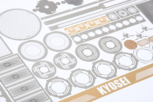
Sample Photo
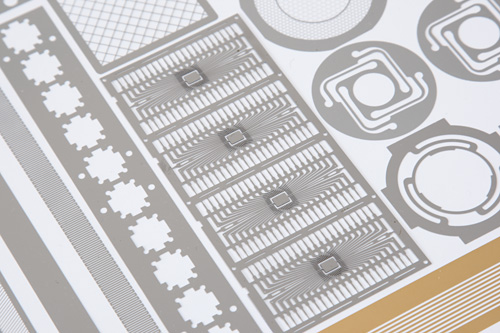
Sample Photo
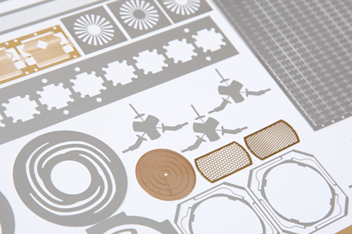
Sample Photo