Back to Fact-Link's Top Page > Electrical / Electronics Parts Production > KYOSEI FACTORY (THAILAND) CO., LTD.

各種金属へのフォトエッチングによる微細・精密加工

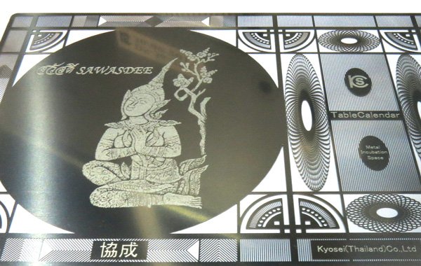
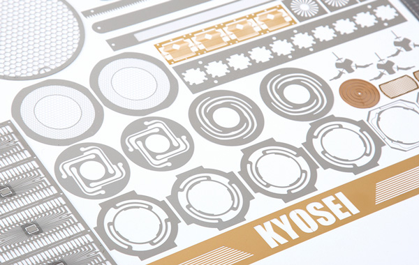
Photo Etching technology is used in high-precision parts for electronics field which could be controlled in the micron millimeteters level. KFT have challenge to study technology for increased accuracy for the future.

協成は東南アジア地域で唯一、金属箔へのフォト・エッチング加工を専業とする部品製造メーカーです。
最先端エレクトロニクス分野の進化と共に長年培われた高い技術力と高度に管理された生産技術で
タイ国内から日本・ASEAN域内へQCD バランスで高精度な製品を提供します。

​また金属加工品への表面処理・塗装・特殊メッキ・電解/化学研磨等、
お客様のニーズに合わせた各種表面処理も対応します。

Etching characteristics

Unnecessity DIE fee for mass product

Photo Etching does not require expensive DIE for product.

Quick Delivery

After 3days we can finish product Wide variety of materials inventory.

加工MOQ:1個、納期:最短3日

Burr-free & Half thickness control

Burr do not occur by Etching product part.Photo Etching is can be control half thickness control.

Material

SUS / Copper alloy / Carbon steel /
Special metal excluding aluminum

Thickness

t=0.010-1.5mm タイ工場加工実績品 各種在庫有り。


SUS/銅合金は0.1mm単位で各種板厚在庫を確保しています。
金属箔材料、少量販売も可能です。お気軽にお問合せ下さい。

Photo Etching Process  >

Product Sample  >

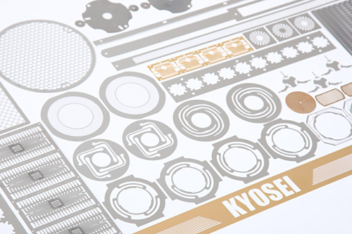
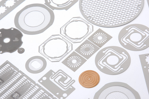
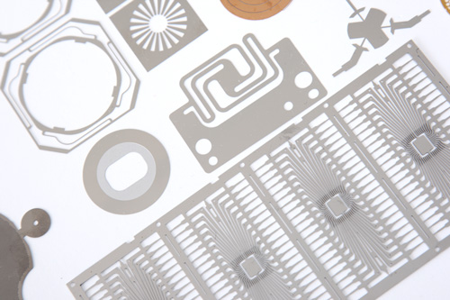
Major usage of etching products

Electrical parts
Electronic parts

Encoder, Lead frames, Metal filters, Spacers, Earth plate, Yokes, Heater shield plate, Metal masks

Parts for OA devices
Parts for optical devices

Leaf springs, Grid plates, Encoder, Shutter, Aperture, Douser, Precision leaf springs, 絞り板
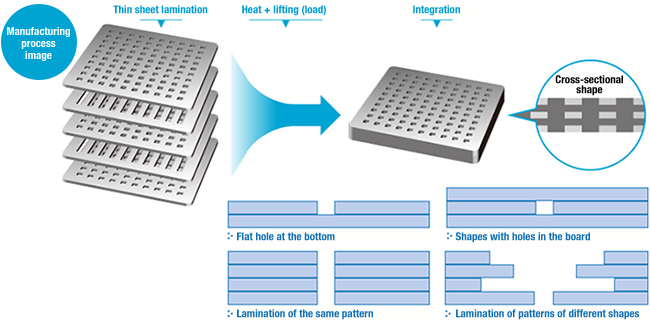
Diffusion Bonding

主にSUS系の素材を積層し立体的な形状を作る技術です。用途に合わせ自在な形状での製造が可能です。
Joinable materials : SUS, Copper Alloy


Latest Update 10 Mar 2025
Powered by Fact-link.com
Back to Fact-Link's Top Page